CORE PRODUCT 02 / WAFER AOI
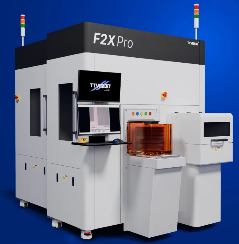
F2X Series
Wafer AOI & 3D Metrology
A wafer inspection family covering surface defects, probe marks, sawing and bump defects, with dedicated models for 3D bump metrology and subsurface micro-crack inspection.
8-inch & 12-inch formatsAI-assisted classificationSECS/GEM
- Rule-based and AI-based dual gate detection algorithms
- Multi-magnification inspection and multiple illumination channels
- Vibration-isolated granite stage and intuitive review software
- Dual-arm cleanroom robot; gripper transfer for mounted wafers
| Model | Inspection focus |
|---|---|
| F2X Pro | Wafer & sawn wafer surface AOI |
| F2X Pro+ | 2D surface inspection & 3D bump metrology Bump height range: 5–250 µm |
| F2X S3i | Subsurface micro-cracks on sawn wafers |
Pro / Pro+: 2X, 5X and 10X surface inspection; listed rates of 60, 35 and 15 WPH respectively. S3i is dedicated to mounted wafers, including invisible, bottom, side and inner cracks. Model performance depends on inspection mode and configuration.